Any molecular nanotechnology must be based on chemistry, and the field has taken a number of directions. Organic chemists have produced a wide variety of small structures, including testable two junction computer devices [Reed 1998][Rawlett 1999]. Biotechnology has been used to create a wide variety of systems, including 2D crystal patterns of DNA [Winfree 1998], modified copies of biological molecular motors [Montemagno 1999] , and covalently bonded molecular tubes with precise radius [Ghadiri 1993]. Fullerene nanotechnology development has produced transistors [Tans 1998][Martel 1998] and diodes [Collins 1997]. A wide variety of theoretical studies have examined the properties of many other potential devices, including fullerene gears [Han 1997][Srivastava 1997], bearings [Tuzun 1995a][Tuzun 1995a], and three junction electrical devices [Menon 1997].
Progress in molecular nanotechnology can be reasonably expected to enable radical improvement in a wide variety of aerospace systems and applications. Computer technology will probably be the first to feel the molecular nanotechnology revolution, with substantial advantages to the aerospace industry. Theoretical and numerical studies suggest that 1018 MIPS computers [Drexler 1992a] and 1015 bytes/cm2 write once memory [Bauschlicher 1997] are possible. It may also be possible to build safe, affordable vertical take-off and landing aircraft to replace personal automobiles [Hall 1999] and eliminate the need for most roads. From [Srivastava 1999b]:
The paper is divided into sections reviewing molecular nanotechnology itself (atomic scale control and imaging, programmable matter, molecular machines, and replication), some of the chemistry behind molecular nanotechnology (organic chemistry, biotechnology, and fullerene nanotechnology), and some of the major challenges and opportunities ahead.

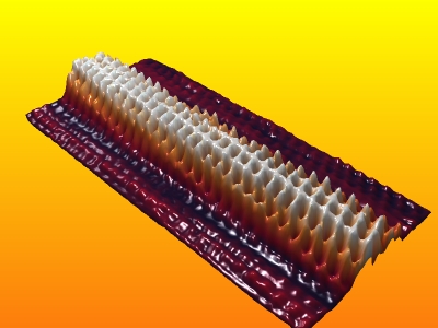
| Atomically precise image of a carbon nanotube. Note the helical winding. For small diameter tubes, the helical winding determines the electrical characteristics of the tube. Image due to [Dekker 1999]. Used with permission. |
Scanning tunneling microscopy (STM) involves the tunneling of electrons through vacuum from the tip of the STM to the sample. STM is very accurate but can only interact with conductors. STMs can also be used to manipulate molecules. For example:
| These carbon nanotubes were cut by applying a voltage pulse to an STM tip. The images show a nanotube before and after cutting. Images due to [Dekker 1999]. Used with permission. |
Atomic force microscopes (AFM) usually sense Van der Walls forces from a surface. This allows measurement of nonconductive surfaces as well as operation in air and liquid. If a chemically active molecule is placed on the tip, then an AFM can be used to measure chemical forces between the tip and a surface. [Frisbie 1994] introduced the term "chemical force microscopy" when they coated an AFM tip with a hydrophilic monolayer and imaged a surface patterned with hydrophobic and hydrophilic molecules. While the surface appeared smooth to an unmodified AFM tip, [Frisbie 1994] was able to measure differences in frictional forces between hydrophobic and hydrophilic portions of the surface, achieving an estimated resolution of about 200 nm. To achieve higher resolution, and measure the interaction of individual molecules with a surface, a sharper tip is necessary. [Dai 1996] was able to attach carbon nanotubes to SPM tips to achieve atomic precision. [Wong 1998] subsequently used open ended carbon nanotubes, covalently functionalized with several different molecules, to image a chemically varied surface achieving a lateral chemical resolution of approximately 3 nm, "... significantly better than ... obtained with the use of Si and Si3N4 (15 nm) or multi-walled-carbon-nanotube tips (8 nm)" [Wong 1998]. Scanning the sample with different functional groups on the tip resulted in distinctly different images and the differences could be explained on the basis of chemical affinity between the tip and the surface. Since both closed and open carbon nanotubes may be functionalized in many ways, Modified nanotube probes may someday perform extremely well-controlled chemistry at precise locations and use applied forces to overcome reaction barriers.
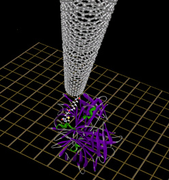
| A model of a carbon nanotube used as a probe with biotin binding to streptavidin. Image from Dr. Lieber's website http://magic.harvard.edu/research.html. Used with permission. |
Carbon nanotubes (see the section on Fullerene Nanotechnology below) have been manipulated in several recent studies. [Falvo 1999] was able to demonstrate rolling and sliding of carbon nanotubes pushed by an AFM on mica and graphite surfaces. Stick-slip behavior was observed in the force curves for rolling. [Skidmore 1999] was able to build and observe a variety of carbon nanotube structures by placing multiple SPM tips around a sample within view of scanning and transmission electron microscopes. Electron beam deposition was used to build up structures in localized positions from a gas feedstock. The SPM tips could manipulate the carbon nanotubes and cut them. Three-dimensional structures were built and carbon nanotubes were weaved around posts. [Skidmore 1999] is probably the most sophisticated manipulation of carbon nanotubes to date. The sample and apparatus used for manipulation can be moved from microscope to microscope to take advantage of the properties of particular devices.
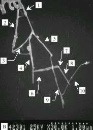
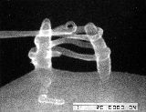
| Two artificial nanotube arrangements built by Zyvex, Inc. [Skidmore 1999]. The image on the left shows a nanotube scaffolding. Numbers show the ordering of tube attachment. The image on the right shows nanotube weaving. Images used with permission. |
Mechanical manipulation of carbon nanotubes may also lead to a new form of chemistry. [Falvo 1997] was able to repeatedly bend individual multi-walled carbon nanotubes using a interactively-controlled AFM. This manipulation demonstrated the high strength of carbon nanotubes and the formation of kinks when nanotubes are bent. [Srivastava 1999a] computationally predicted that mechanically induced strain leads to regions of enhanced chemical reactivity as carbon atoms change from a stable sp2 (planar) configuration with three neighbors towards a less stable sp3 (pyramidal) configuration with three neighbors and one radical site in regions of greatest strain. [Srivastava 1999a] presents some experimental data that support, but do not confirm, this prediction. If the prediction holds true, mechanical manipulation might be used to induce strain at desired locations along a carbon nanotube leading to selective attachment of functional groups from a reagent bath at those locations.
In a spectacular example of the power of programmable matter, [Schwarze 1999] use a portion of the HIV viral protein to insert a wide variety of proteins into mammalian cells and live mice. Typically, only small therapeutic molecules can enter cells. [Schwarze 1999] attached an 11 amino acid protein transaction domain from the HIV virus to a variety of proteins. The protein transaction domain apparently enters cells directly through the lipid bilayer component of the cell membrane, not through special pathways. The desired proteins were denatured (unfolded), attached to the transaction domain, and then passed into the cell where the cell's protein folding machinery folded the protein into a potentially active form. Since essentially any polypeptide can be made by sending the sequence specification and a credit card number to any of several companies, it may be possible to engineer proteins to attack specific points in the molecular life-cycle of disease organisms and deliver these proteins into infected cells. With a polypeptide sequencer and related biotech systems on-board a space station, when disease strikes the necessary medicine for that particular pathogen could be manufactured on-board from instructions sent up from the ground. This would reduce the need for large stocks of medicine for every possible contingency. The same protein sequencer could also be used for research purposes.
DNA has been used to build 3d topological shapes [Chen 1991][Zhang 1994], stiff structures [Li 1996], crystals [Winfree 1998], and even a molecular machine [Mao 1999a]. This was accomplished by taking advantage of DNA's hydrogen-bonded complementarity and biotechnology's ability to produce almost any DNA sequence desired. By cleverly choosing the sequence of base pairs, Seaman's laboratory has produced a remarkable variety of structures, for example:
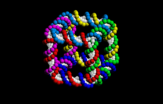
| DNA cube made from six different cyclic strands. The DNA backbones are shown in different colors. Each nucleotide is represented by a single colored dot for the backbone and a single white dot for the base. To get a feeling for the molecule, follow the red strand around its cycle. Each edge of the cube is a piece of double helical DNA containing two turns of the double helix. Image due to Ned Seeman [Chen 1991] and http://seemanlab4.chem.nyu.edu/nano-cube.html. Used with permission. |
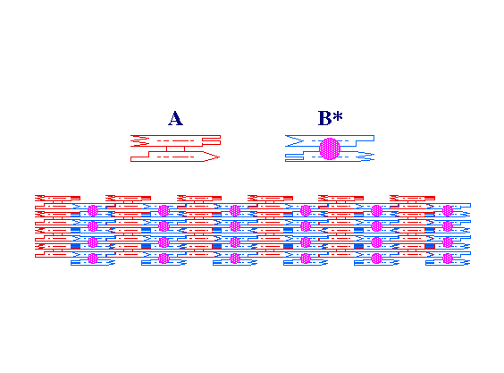
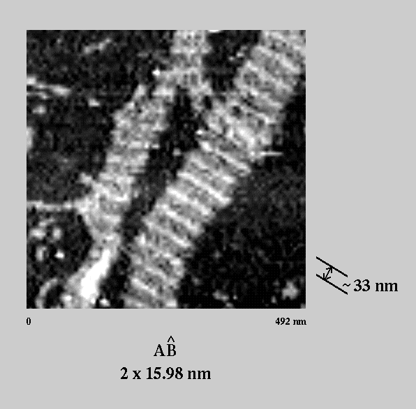
| Two DNA double crossover molecules A and B* use complementarity between their sticky ends (represented as geometric complementarity) to form a two dimensional crystal. The B* molecules contain DNA hairpins that project out of plane to allow AFM discrimination. The molecules are approximately 4 nm wide, 16 nm long and 2 nm thick. When these tiles are mixed in solution, they form hydrgen bonded 2-D arrays several microns long and hundreds of nanometers wide. The rows of hairpins appear as stripes separated by ~32 nm when imaged by AFM (below) [Mao 1999b]. Images due to Ned Seeman from http://seemanlab4.chem.nyu.edu/two.d.html. Used with permission. |
[Montemagno 1999], building on the work of [Noji 1997], is attempting to integrate the biological motor F1-ATPase with nano-electro-mechanical systems to create a new class of hybrid nanomechanical devices. ATPase is used by mitochondria to synthesize ATP from ADP, phosphate, and proton gradients. ATP is the primary energy source of our bodies. The F1 portion of ATPase has a sub-unit that turns during synthesis. This rotation can be reversed by separating the F1 sub-unit from the rest of the protein and feeding the sub-unit ATP. F1-ATPase can generate >100 pN, has a measured rotational velocity of 3 r.p.s. under load, and a diameter of less than 12 nm. These characteristics suggest that F1-ATPase could manipulate currently manufacturable nanomechanical structures. Since the human body produces ample quantities of ATP, an implantable sensor in an astronaut's body operated by F1-ATPase would require no other power source. Such sensors could provide medically important data on an astronaut's health indefinitely.
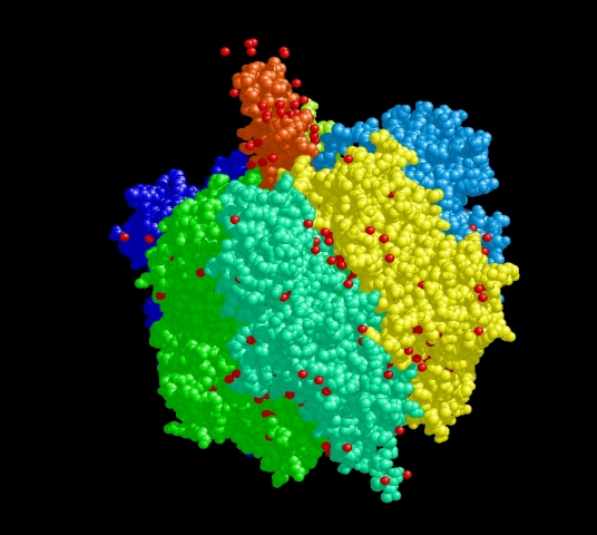
| F1-ATPase [Abrahams 1994]. The orange sub-unit rotates. The six sub-units in shades of yellow, green and blue rock back and forth sequentially as ATP is hydrolyzed [Elston 1998]. |
Another biological molecular motor, kinesin, was deposited on polymer films in order to guide the motion of microtubules on surfaces [Dennis 1999]. Kinesin has also been used to manipulate 10 x 10 x 5 µm silicon microchips. These microchips were translated, rotated, and in a few instances turned over by large numbers of kinesin motors [Limberis 1999]. Normally, kinesin motors operate on microtubule "tracks" inside cells. From [Limberis 1999]:
[Mao 1999a] created an artificial two-state molecular machine from DNA. [Mao 1999b] connected two stiff double-crossover DNA molecules [Li 1996] with a strand of DNA that could assume either a right-handed helix (B-DNA) or a left-handed helix (Z-DNA) conformation depending on certain characteristics of the solution the molecules were in. By changing the solution and forcing the connecting DNA strand to wind in the opposite direction, the stiff portions were forced to move. This movement was recorded by placing dye molecules on each stiff segment. "The switching event induces atomic displacements of 20-60 angstroms" [Li 1996]. This experiment was controlled by running the same test on similar DNA molecules where the connecting segment was not capable (due to the sequence used) of assuming the Z-DNA conformation. These molecules did not change conformation when the solution changed.
A very interesting non-biological partly-molecular machine has been fabricated by Philip Kim and Charles M. Lieber [Kim 1999]. They attached a nanotube bundle to each of two independent electrodes deposited on a pulled glass micropipette. This enables independent control of charge on each nanotube. When the nanotubes are oppositely charged they can be induced to close like tweezers - nanotweezers - thereby enabling nanoscale objects to be held and manipulated in three dimensions. The nanotube nanotweezers have been used to manipulate and measure the electrical properties of nanoclusters and nanowires.
[Freitas 1980] studied a hypothetical 100-ton self-replicating lunar factory with access only to local resources and established materials processing techniques. This study assumed macroscopic machines, not nanotechnology. While a number of self-replication strategies are possible, perhaps the most practical is for a computer to interpret a set of instructions and control a robot to make a copy of itself, a technique originally proposed by von Neuman. This has the added virtue that the instructions can be changed so the replicator can make something else. If the computers themselves are provided using mass production technologies instead of replication, then the replication can be limited and controlled to avoid the most serious runaway scenarios.
From [Freitas 1980]:
p(t) -- population at time t
g -- generation time (seconds to replicate)
a -- "alacrity" primitive assembly operations
per second
s -- size in primitive operations to construct
n -- number of primitive operating units
Then ![]() and
and  ."
[Hall 1998] then investigated the implications of such a model, particularly
with regards to bootstrapping ever more capable replicators. From this
analysis, he derived a potential system architecture detailed in the following
figure:
| "System diagram for the bootstrap path of a self-replicating manufacturing system. Each subsystem in a blue line (as well as the entire system) meets the self-replicating system criterion." The turquoise ellipses represent components. The black arrows represent material or information flows. The red arrows represent fabrication. By Hall's criteria, a system is self-replicating if every turquoise ellipse has an incoming red arrow and all red arrows originate from a turquoise ellipse. Image from [Hall 1998]. Used with permission. |
[Freitas 1980] suggested several applications for space based self-replicating
manufacturing systems (SRS). Such systems might use solar energy and lunar
or asteroidal materials. Asteroidal materials might be delivered by large
numbers of fully automated solar sail powered spacecraft that capture and
return small (~1 m diameter) meteoroids [Globus 1999]. From [Freitas 1980]
:
Any technology employing replicators will require mechanisms to insure
safe use. Existing replicators such as bacteria and viruses cause severe
problems; for example, human death rates exceeding 50 percent in unprotected
populations. The possibility of accidental or deliberate misuse of replicators
must be addressed, preferably before problems arise. One threat is the
production and release of artificial infectious agents, an extension of
the germ warfare in development today. Current efforts to address germ
warfare defense could be extended to address artificial threats. Control
approaches include only designing replicators that require crucial components
to be built by other means, not allowing replicators to program themselves,
and only developing replicators that function solely in artificial environments,
such as a helium atmosphere. A second threat is the rapid production of
large quantities of armaments using the exponential growth capability of
replicators. Continuous, high resolution, and ubiquitous monitoring may
be required to meet this threat. Unfortunately, it may be possible to develop
dangerous replicators in great secrecy. Note that the Iraqi government
hid their germ warfare program from onsite inspection for years until a
defector blew the whistle. Thus, it is probably extremely important to
develop molecular nanotechnology out in the open with universal access
to results. Requiring free publication of at least government funded results
on the World Wide Web is one strategy. Many molecular nanotechnology scientists
follow this practice today.
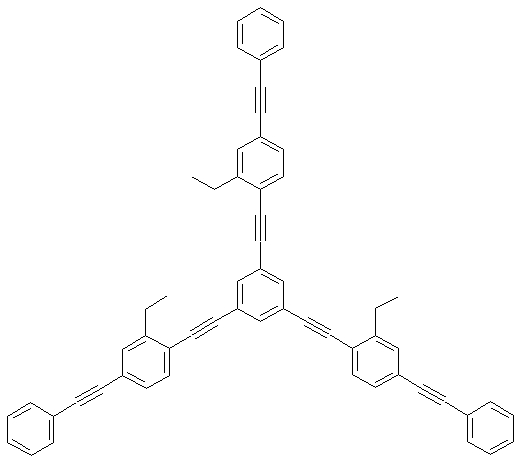
[Tour 1998] synthesized a number of organic molecules based on benzene and investigated their computational possibilities. Since these molecules can be controllably synthesized in vast numbers, they have great potential as building blocks for nanoelectronic circuits. Noting that transporting electrons through networks of such molecules would generate unacceptable amounts of heat, [Tour 1998] proposed using small changes in electron density to pass information and perform logic functions. While [Tour 1998] discussed quantum calculations to support the notion of using electron density changes for logic, it's unclear how the small signals proposed could be distinguished from thermal noise [Bauschlicher 1999], an issue not addressed in [Tour 1998]. Nonetheless, if these molecules can be connected appropriately, noise problems overcome, and a variety of other problems conquered, these molecules could lead to molecular computers operating at femtosecond time scales.
|
|
[Reed 1998] devised a novel mechanically controllable break junction to staticly test benzene-1,4-dithiol molecules, a component of the devices in [Tour 1998]. Using this device, [Reed 1998] was able to reproducibly measure the conductance of single molecules. The observed resistance, approximately 22 Mohm and 13 Mohm depending on the bias, was within the error bounds derived from measurements on an ensemble of similar molecules.
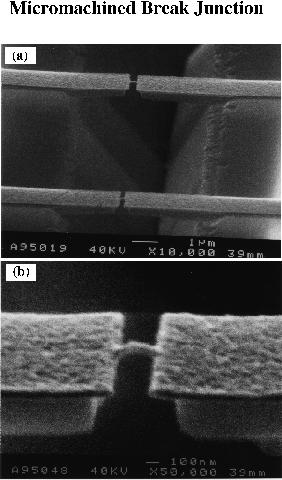
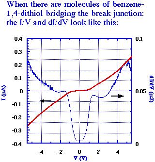
Images used with permission [Reed 1998].
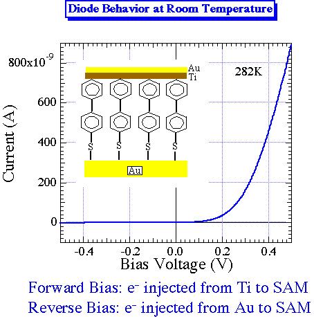
[Reed 1998] also built a device to directly measure the conduction through a small group of organic molecules using self-assembly and semiconductor fabrication techniques. This device was used to measure a diode-like molecule:
[Ellenbogen 1999] designed a one bit adder out of molecular wires [Tour 1998] with chemical groups added to implement molecular resonant tunneling diodes and molecular rectifying diodes. These two diodes are sufficient to implement AND, OR and XOR logic elements. In turn, these logic elements are sufficient to implement a wide variety of devices, including adders. The full adder would occupy approximately 25 nm by 25 nm of a surface, approximately one million times smaller than current electronics. However, such a circuit has no gain and probably would not work well in an extended system. There is also reason to believe that the clock rate of these molecular devices would be quite low, possibly slower than current electronics. Quantum calculations suggest that each component of the adder would work properly, but the entire adder may or may not work due to coupling between the devices. Nonetheless, [Ellenbogen 1999] is a substantial step towards molecular electronics.
One problem with these molecular electronics devices is the low levels of current measured experimentally [Reed 1998]. However, [Emberly 1998] used computation to suggest that the low levels of current are due to the contact with the gold leads, not the molecule itself. In fact, molecular wires modeled with strong coupling to the leads were found to have currents orders of magnitude better than observed experimentally. Molecular wire current computed assuming weak coupling matched experiment [Emberly 1998]. If these computations turn out to reflect reality, then a different choice of contacts may lead to higher currents and more practical computer components based on organic chemistry.
Another problem with the molecules discussed so far is that they contain no fused rings and are thus fairly floppy. [Hush 1998] proposed using porphyrin chemistry with fused ring connectors for molecular electronics.

[Hush 1998] noted that any molecular family used for molecular electronics should have several properties, including:
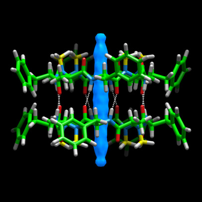
| "Crystal structure of cyclo-[(L-Phe-D-N-Me-Ala)4] including a partially ordered water centered in the cyclic peptide" [Hartgerink 1996]. Image used with permission. |
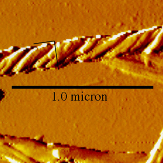
| "Atomic Force Microscopy image of the self-assembling peptide nanotube formed by the cyclic peptide cyclo-[(L-Glu-D-Ala)4] . The nanotube shown here has an unusual right handed super helical form" [Hartgerink 1996]. Image used with permission. |
[Pum 1999] used crystalline bacterial cell surface layer (S-layer) proteins to assemble into two-dimensional arrays on silicon wafers and other surfaces. S-layer proteins, of which there are many, form surfaces on the outside of cells. [Pum 1999] used these proteins to position metals on a surface and then removed the protein by heating. Functional groups were repeated with the periodicity of the S-layer lattice (approximately 10nm) and this can be used to "... induce the formation of inorganic nanocrystal superlattices (e.g. CdS, Au, Ni, Pt, or Pd) with a broad range of particle sizes (5 to 15nm in diameter), interparticle spacings (up to 30nm) and lattice symmetries (oblique, square or hexagonal) as required for molecular electronics and non-linear optics" [Pum 1999]. S-layers can have oblique, square or hexagonal lattice symmetry with a unit cell of 3 to 30nm. S-layers are usually 5 to 10 nm thick with 2 to 8 nm pores.
While living things have shown us something of what nanotechnology might produce, most biomolecules are far too fragile for many aerospace environments. For example, it is unlikely that proteins or DNA can survive in rocket engines. One newly-discovered class of molecules, fullerenes, particularly carbon nanotubes [Iijima 1991], built from graphene sheets curved into a wide variety of close shapes, may lead to tougher, higher-temperature materials that can survive in a vacuum and other harsh environments. Fullerenes also have certain advantages for electronic applications.
Since [Globus 1998b] was written, substantial progress has been made in manufacturing, controlling, and understanding carbon nanotubes and related structures. In particular, some of the predicted electronic properties of small-diameter single-walled carbon nanotubes have been confirmed, and a few devices have been built and tested. In addition, new numerical predictions have been made of ever more detailed devices and realistic systems. There has also been progress controlling the manufacturing process and in connecting carbon nanotubes to electronic components built by more conventional manufacturing techniques.
When a metallic and a semiconducting tube are joined, a device may be formed. For example, [Collins 1997] reports using an STM to explore the local electrical characteristics of single-wall carbon nanotubes. As the tip moved along the length of the nanotubes, well-defined positions were found where the current changed abruptly, in some cases exhibiting near-perfect rectification. These observations were consistent with localized, on-tube nanodevices predicted theoretically [Chico 1996].
[Service 1999] reported that Zettl, McEuen, and Fuhrer discovered an excellent diode formed from a pair of carbon nanotubes that crossed and didn't touch any neighbors. The properties of the diode were determined by attaching gold electrodes and passing current through the device. Unfortunately, the same article reports that Zettl and Collins discovered that both individual metallic carbon nanotubes and bundles are extremely noisy electrical conductors. The cause of the noise is currently unknown, but may be due to the impurities in the sample examined. If this is true, then the chemistry influences carbon nanotube electronic properties, which may be beneficial if it can be controlled.
[Tans 1998] reported the construction and testing of a field-effect transistor (a three-terminal switching device) consisting of a single semiconducting single-walled carbon nanotube in contact with metal electrodes. [Tans 1998] applied a large number of carbon nanotubes to a surface with pre-fabricated platinum electrodes placed on a silicon surface with an intervening 300 nm silicon oxide layer. [Tans 1998] found and measured over 20 individual tubes that were found draped over platinum electrodes. Some of these tubes exhibited metallic behavior. Others acted as the semiconductor component of a field-effect transistor. In other words, when a bias was applied to the gate electrode, the carbon nanotube effectively changed from an insulator to a conductor. This device, unlike diodes, exhibits gain. Gain is necessary for fan-out, making up for losses, and is considered essential for practical devices. The estimated maximum frequency of the transistor is about 10 THz, achievable in part by reducing the width of the silicon dioxide surface to about 5 nm. [Tans 1998] was able to use standard bulk material models to qualitatively describe the carbon nanotube based transistor. Unlike the molecules used in [Ellenbogen 1999], there is currently no general methodology for controlling the production of carbon nanotubes with the precision necessary to devise electronic circuits. Also, carbon nanotubes are somewhat larger than Tour wires. However, if the synthetic challenges can be overcome, the higher current densities allowed and the fact that gain has been demonstrated makes carbon nanotubes a prime candidate for molecular computers.
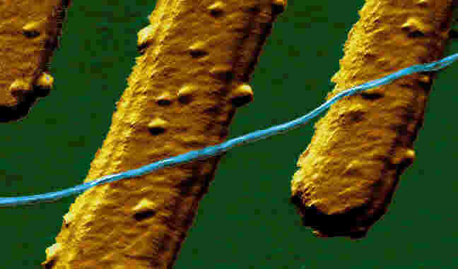
| Single-walled carbon nanotube draped across platinum electrodes [Tans 1998]. Image used with permission. http://vortex.tn.tudelft.nl/~dekker/nanotubes.html. |
[Martel 1998] produced field-effect transistors from single- and multi-walled carbon nanotubes at about the same time. The abstract to this paper is so perfectly written is difficult to improve upon:
Constructing carbon nanotube computers is of no value if they cannot be connected to the outside world. [Zhang 1999] reported a relatively easy mechanism for connecting single walled carbon nanotubes to metals and silicon. [Zhang 1999] brought nanotubes into contact with silicon- and metal-based surfaces in a hard vacuum and heated the surface. The two materials became joined by carbide (a combination of carbon and the silicon or metal). Not only did [Zhang 1999] accomplish this with masses of carbon nanotubes on extended surfaces, they also connected titanium pads with carbon nanotubes. Current between titanium pads connected by carbon nanotubes varied linearly with voltage and resistance between them dropped dramatically after the heat treatment, indicating that a good electrical connection was created. [Zhang 1999] also used the technique to attach a bundle of single wall nanotubes to a titanium STM tip. Note that [Anantram 1999] predicted computationally that electron transport between carbon nanotubes and a substrate should be substantial, particularly if nanotube defects exist close to the cap.
For the most part, interesting carbon nanotube structures are found by producing large numbers of tubes in a relatively uncontrolled environment and examining the results molecule-by-molecule until an interesting structure is found. [Cassell 1999] reported a notable exception to this pattern. [Cassell 1999] built single-walled nanotube bridges suspended "... from catalyst material placed on top of regularly patterned silicon tower structures." Single-walled carbon nanotubes are grown from metal catalysts. The silicon towers, topped by catalyst metals, were constructed using conventional techniques, then carbon nanotubes were grown from the catalyst. Most of the tubes fell over the edge of the catalyst when they become long enough. Those that fell onto an adjacent tower remained suspended over the substrate between the two towers. By controlling the location of the towers, specific patterns of carbon nanotubes were synthesized. For example:
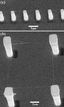
| Carbon nanotube "power line" and a square from [Cassell 1999]. The large white objects are catalyst-tipped towers. The thin lines are carbon nanotubes. Image used with permission. |
[Abrahams 1994] J. Abrahams, Andrew G. W. Leslie, Rene Lutter and John E. Walker, "Structure at 2.8 Angstrom Resolution of F1-ATPase from Bovine Heart Mitochondria," Nature, Volume 370, pages 621-628, 25 August 1994.
[Anantram 1999] M. P. Anantram and T. R. Govindan, "Transport through carbon nanotubes with polyhedral caps", submitted for publication.
[Avouris 1999] Ph. Avouris, T. Hertel, R. Martel, T. Schmidt, H.R. Shea, and R.E. Walkup, "Carbon Nanotubes: Nanomechamics, Manipulation, and Electronic Devices" Applied Surface Science, volume 141, pages 201-209.
[Bauschlicher 1997] Charles W.Bauschlicher Jr., Alessandra Ricca and Ralph Merkle, "Chemical storage of data," Nanotechnology, volume 8, number 1, March 1997, pages 1-5.
[Bauschlicher 1999] Charles W.Bauschlicher Jr., personal communication.
[Burger 1980] J. Burger, D. Brill, and F. Machi, "Self-Reproducing Programs," Byte, volume 5, June 1980.
[Cagin 1998] T. Cagin, A. Jaramillo-Botero, G. Gao, and W. A. Goddard III , "Molecular Mechanics and Molecular Dynamics Analysis of Drexler-Merkle Gears and Neon Pump," Nanotechnology, volume 9, pages 143-152.
[Cassell 1999] Alan M. Cassell, Nathan R. Franklin, Thomas W. Tombler, Emery M. Chan, Jie Han, and Hongjie Dai, "Directed Synthesis of Free-Standing Single Walled Carbon Nanotubes," Journal of the American Chemical Society, volume 121, pages 7975-7976.
[Chen 1991] J. Chen and Nadrian C. Seeman, "The Synthesis from DNA of a Molecule with the Connectivity of a Cube," Nature, volume 350, pages 631-633.
[Chico 1996] L. Chico, Vincent H. Crespi, Lorin X. Benedict, Steven G. Louie and Marvin L. Cohen, "Pure Carbon Nanoscale Devices: Nanotube Heterojunctions," Physical Review Letters, volume 76, number 6, 5 February 1996, pages 971-974.
[Collier 1999] C. P. Collier, E. W. Wong, M. Belohradský, F. M. Raymo, J. F. Stoddart, P. J. Kuekes, R. S. Williams, J. R. Heath, "Electronically Configurable Molecular-Based Logic Gates," Science, volume 285, number 5426, 16 July 1999, pages 391-394.
[Collins 1997] Philip G. Collins, A. Zettl, Hiroshi Bando, Andreas Thess, R. E. Smalley, "Nanotube Nanodevice," Science, volume 278, number 5335, 3 October 1997, pages 100 - 102.
[Dai 1996] H. Dai, J. H. Hafner, A. G. Rinzler, D. T. Colbert and R. E. Smalley, "Nanotubes as Nanoprobes in Scanning Probe Microscopy," Nature, volume 384, pages 147-151.
[Dekker 1999] Cees Dekker, WWW page http://vortex.tn.tudelft.nl/~dekker/nanotubes.html.
[Dennis 1999] J. Dennis, J. Howard, and V. Vogel, "Molecular Shuttles: Drected Motion of Microtubules Along Nanoscale Kinesin Tracks," submitted to Nature.
[Dresselhaus 1995] M. S. Dresselhaus, G. Dresselhaus and P. C. Eklund, Science of Fullerenes and Carbon Nanotubes, Academic Press.
[Drexler 1992a] K. Eric Drexler, Nanosystems: Molecular Machinery, Manufacturing, and Computation, John Wiley & Sons, Inc..
[Drexler 1992b] K. Eric Drexler, Journal of the British Interplanetary Society, volume 45, number 10, pages 401-405.
[Eigler 1990] D. M. Eigler and E. K. Schweitzer, "Positioning Single Atoms with a Scanning Tunneling Microscope," Nature, volume 344, page 524.
[Ellenbogen 1999] James C. Ellenbogen, J. Christopher Love, "Architecture for Molecular Electronic Computers: 1. Logic Structures and an Adder Built from Molecular Electronic Diodes," MP 98W0000183, July 1999, MITRE, McLean, Virginia.
[Elston 1998] Timothy Elston, Hongyun Wang, and George Oster, "Energy Transduction in ATP Synthase," Nature, volume 391, 29 January 1998, pages 510-513.
[Emberly 1998] Eldon Emberly and George Kirczenow, "Electrical Conductance of Molecular Wires," Nanotechnology, volume 10, number 3, September 1999, pages 285-289.
[Falvo 1997] M. R. Falvo, G.J. Clary, R.M. Taylor II, V. Chi, F.P. Brooks Jr., S. Washburn and R. Superfine, "Bending and buckling of carbon nanotubes under large strain," Nature, volume 389, pages 582-584.
[Falvo 1999] M. R. Falvo, R. M. Taylor II, A. Helser, V. Chi, F. P. Brooks Jr., S. Washburn, and R. Superfine, "Rolling and sliding of carbon nanotubes", Nature, volume 397, pages 236-238.
[Freitas 1980] Robert A. Freitas, Jr. and William P. Gilbreath, editors, "Advanced Automation for Space Missions," Proceedings of the 1980 NASA/ASEE Summer Study; sponsored by the National Aeronautics and Space Administration and the American Society for Engineering Education, NASA Conference Publication 2255.
[Frisbie 1994] C. Daniel Frisbie, Lawrence F. Rozsnyai, Aleksandr. Noy, Mark S. Wrighton, Charles M. Lieber, "Functional Group Imaging by Chemical Force Microscopy," Science, volume 265, 30 September 1994, pages 2071-2074.
[Ghadiri 1993] M. R. Ghadiri, J. R. Granja, R. A. Milligan, D. E. McRee, N. Khazanovich, "Self-Assembling Organic Nanotubes Based on a Cyclic Peptide Architecture," Nature, volume 366, pages 324-327. See http://www.scripps.edu/pub/ghadiri/html/research.html.
[Gimzewski 1997] J. K. Gimzewski, T. A. Jung, M. T. Cuberes, and R. R. Schlittler, "A Scanning Tunneling Microscopy of Individual Molecules: Beyond Imaging," Surface Science, 386 (1-3), pages 101-114.
[Gimzewski 1998] J. K. Gimzewski, C. Joachim, R. R. Schlittler, V. Langlais, H. Tang, and I. Johannsen, "Rotation of a Single Molecule within a Supramolecular Bearing," Science, volume 281, 24 July 1998, pages 531-533.
[Globus 1998a] "Aerospace applications of molecular nanotechnology," Al Globus, David Bailey, Jie Han, Richard Jaffe, Creon Levit, Ralph Merkle and Deepak Srivastava, The Journal of the British Interplanetary Society, volume 51, pages 145-152.
[Globus 1998b] "Machine Phase Fullerene Nanotechnology," Al Globus, Charles Bauschlicher, Jie Han, Richard Jaffe, Creon Levit, Deepak Srivastava, Nanotechnology, volume 9, number 2, September 1998, pages 192-199.
[Globus 1999] Al Globus, Bryan Biegel, and Steve Traugott, "AsterAnts: A Concept for Large-Scale Meteoroid Return and Processing Using the International Space Station," Space Frontier Conference 8, Los Angeles California, September 1999.
[Hall 1998] J. Storrs Hall, "Architectural Considerations for Self-replicating Manufacturing Systems," Sixth Foresight Conference on Molecular Nanotechnology, Sunnyvale California, November 1998.
[Hall 1999] J. Storrs Hall, personal communication.
[Han 1997] Jie Han, Al Globus, Richard Jaffe and Glenn Deardorff, "Molecular Dynamics Simulation of Carbon Nanotube Based Gears," Nanotechnology, volume 8, number 3, 3 September 1997, pages 95-102.
[Hunt 1994] A. Hunt, F. Gittes, and J. Howard, "The Force Exerted by a Single Kinesin Molecule against a Viscous Load," Biophysical Journal, volume 67, August 1994, pages 766-781.
[Hartgerink 1996] Jeffrey Dale Hartgerink, http://www.scripps.edu/pub/ghadiri/html/research.html.
[Hay 1980] Louise Hay, "Self-Reproducing Programs," Creative Computing, volume 6, July 1980, pp.134-136.
[Heath
1998] James R. Heath, Philip J. Kuekes, Gregory S. Snider, R. Stanley
Williams, "A Defect-Tolerant Computer Architecture: Opportunities for
Nanotechnology," Science, volume 280, number 5370, 12 June 1998,
pages 1716-1721.
[Hush 1998] Noel S. Hush, Jeffrey R. Reimers, Lachlan E. Hall, Lesley A. Johnson, and Maxwell J. Crossley, "Optimization and Chemical Control of Porphyrin-Based Molecular Wires and Switches," Annals of the New York Academy and Sciences, Volume 852, Molecular Electronics: Science and Technology, edited by Ari Aviram and Mark Ratner, pages 1-21.
[Hush 1999] Noel S. Hush, personal communication.
[Iijima 1991] Sumio Iijima, "Helical microtubules of graphitic carbon," Nature, 7 November 1991, volume 354, N6348:56-58.
[Jacobson 1958] Homer Jacobson, "On Models of Reproduction," American Scientist, volume 46, pages 255-284.
[Kim 1999] Philip Kim and Charles M. Lieber, "Nanotube Nanotweezers," Science, accepted for publication.
[Kull 1996] F. Kull, E. Sablin, R. Lau, R. Fletterick, and R. Vale, "Crystal Structure of the Kinesin Motor Domain Reveals a Structural Similarity to Myosin," Nature, volume 380, 11 April 1996, pages 550-555.
[Lee 1996] D. H. Lee, J. R. Granja, J. A. Martinez, K. Severin, M. R. Ghadiri, "A Self-Replicating Peptide," Nature 382, pages 525-28.
[Li 1996] Xiaojun Li, Xiaoping Yang, Jing Qi, and Nadrian C. Seeman, "Antiparallel DNA Double Crossover Molecules As Components for Nanoconstruction," Journal of the American Chemical Society, volume 118, pages 6131-6140.
[Limberis 1999] Loren Limberis, Chih-Hu Ho, and J. Russell Stewart, "Kinesin-powered MicroChemoMechanical Systems (MCMS)," Seventh Foresight Conference on Molecular Nanotechnology, Sunnyvale California, October 1999.
[Mao 1999a] C. Mao, W. Sun, Z. Shen and N.C. Seeman, A DNA Nanomechanical Device Based on the B-Z Transition, Nature, volume 397, pages 144-146.
[Mao 1999b] C. Mao, W. Sun and N.C. Seeman, "Designed Two-Dimensional DNA Holliday Junction Arrays Visualized by Atomic Force Microscopy," Journal of the American Chemical Society, volume 121, pages 5437-5443.
[Martel 1998] R. Martel, T. Schmidt, H. R. Shea, T. Hertel, and Ph. Avouris, "Single- and Multi-Wall Carbon Nanotube Field-Effect Transistors," Applied Physics Letters, volume 73, pages 2447-2449.
[McKendree 1995] Tom McKendree, "Implications of Molecular Nanotechnology: Technical Performance Parameters on Previously Defined Space System Architectures," Fourth Foresight Conference on Molecular Nanotechnology, Palo Alto, California, November 1995.
[Menon 1997] M. Menon and D. Srivastava, "Carbon Nanotube 'T-junctions': Nanoscale Metal-Semiconductor-Metal Contact Devices", Physics Review Letters, volume 79, 4453.
[Montemagno 1999] Carlo Montemagno and George Bachand, "Constructing nanomechanical devices powered by biomolecular motors," Nanotechnology, Volume 10, Number 3, September 1999, pages 225-231.
[Morowitz 1959] Harold J. Morowitz, "A Model of Reproduction," American Scientist, volume 47, pages 261-263.
[Noji 1997] H. Noji, R. Yashuda, M. Yoshida, K. and Kinosita Jr., "Direct observation of the rotation of F1-ATPase," Nature 386, pages 299-302.
[O'Neill 1977] Gerard K. O'Neill, technical director, Space Settlements: A Design Study, NASA SP-413.
[O'Neill 1979] Gerard K. O'Neill, study director, Space Resources and Space Settlements, NASA SP-428.
[Penrose 1959] L. S. Penrose, "Self-Reproducing Machines," Scientific American, volume 200, June 1959, pages 105-114.
[Pum 1999] Dietmar Pum, Angela Neubauer, Erika Gyoervary, Sabine Dieluweit, Uwe B. Sleytr: "S-layer proteins as basic building blocks in a biomolecular construction kit," Seventh Foresight Conference on Molecular Nanotechnology, Sunnyvale California, October 1999.
[Reed 1998] Mark A. Reed, C. Zhou, M. R. Deshpande, C. J. Muller, T. P. Burgn, L. Jones II, and James M. Tour, "The Electrical Measurement of Molecular Junctions," Annals of the New York Academy and Sciences, Volume 852, Molecular Electronics: Science and Technology, edited by Ari Aviram and Mark Ratner, pages 133-144.
[Rawlett 1999] A. Rawlett, J. Chen, Mark A. Reed, James M. Tour, "Advances in Molecular Scale Electronics: Synthesis and Testing of Molecular Scale Resonant Tunneling Diodes and Molecular Scale Controllers," Polym. Mater., Sci. Engin. (Am. Chem. Soc., Div. Polym. Mater.) volume 81, pages 140-141.
[Schwarze 1999] Stephen R. Schwarze, Alan Ho, Adamina Vocero-Akbani, Stephen F. Dowdy, "In Vivo Protein Transaction: Delivery of a Biologically Active Protein into the Mouse," Science, Volume 285, Number 5433, 3 September 1999, pages 1569-1572.
[Service 1999] Robert F. Service, "Raising a Glass to Health and Nanotubes," Science, volume 285, number 5436, 24 Sep 1999, pages 2053-2055.
[Skidmore 1999] George D. Skidmore, Matthew Ellis, and Jim Von Ehr, "Free Space Construction with Carbon Nanotubes," Science and Application of Nanotubes, edited by David Tománek and Richard Enbody, Kluwer Academic Publishers (in press), pages 373-386.
[Srivastava 1997] Deepak Srivastava, "A Phenomenological Model of the Rotation Dynamics of Carbon Nanotube Gears with Laser Electric Fields," Nanotechnology, volume 8, pages 186-192.
[Srivastava 1999a] Deepak Srivastava, Donald W. Brenner, J. David Schall, Kevin D. Ausman, Min Feng Yu, and Rodney S. Ruoff, "Predictions of Enhanced Chemical Reactivity at Regions of Local Conformational Strain on Carbon Nanotubes: Kinky Chemistry," Journal of Physical Chemistry B, volume 103, number 21, pages 4330-4337.
[Srivastava 1999b] Deepak Srivastava, Fedor Dzegilenko, Stephen Barnard, Subhash Saini, Madhu Menon, and Sisira Weeratunga, Handbook of Nanostructured Materials and Nanotechnology, Volume 2: Spectroscopy and Theory, chapter 14: "Carbon-Nanotube-Based Nanotechnology in an Integrated Modeling and Simulation Environment," H. S. Nalwa, editor, Academic Press, pages 665-705.
[Svoboda 1993] K. Svoboda., C. Schmidt, B. Schnapp, and S. Block, "Direct Observation of Kinesin Stepping the Optical Trapping Interferometry," Nature, volume 365, 21 October 1993, pages 721-727.
[Tans 1998] S. J. Tans, A. R. W. Verschueren, and C. Dekker, "Room-Temperature Transistor Based on a Single Carbon Nanotube," Nature, volume 393, 7 May 1998, pages 49-52.
[Tour 1998] James M. Tour, Masatoshi Kozaki and Jorge M. Seminario,. "Molecular Scale Electronics: A Synthetic/Computational Approach to Digital Computing," Journal of the American Chemical Society, volume 120, pages 8486-8493.
[Tuzun 1995a] Robert E. Tuzun, Donald W. Noid and Bobby G. Sumpter, "The Dynamics of Molecular Bearings," Nanotechnology, volume 6, pages 64-74.
[Tuzun 1995b] Robert E. Tuzun, Donald W. Noid and Bobby G. Sumpter, "Dynamics of a Laser Driven Molecular Motor," Nanotechnology, volume 6, pages 52-63.
[Unger 1999] Eberhard Unger, Roland Stracke, Jörg Burgold, Hans-Joachim Schacht, Konrad J. Böhm, "Geometrical and temporal factors determining kinesin-dependent microtubule motility in vitro," Seventh Foresight Conference on Molecular Nanotechnology, Sunnyvale California,. October 1999.
[Winfree 1998] E. Winfree, F. Liu, L. A. Wenzler, and N. C. Seeman, "Design and Self-Assembly of Two-Dimensional DNA Crystals," Nature, volume 394, pages 539-544.
[Wong 1998] S.S. Wong, A.T. Woolley, E. Joselevich, C.L. Cheung and C.M. Lieber, "Covalently-Functionalized Single-Walled Carbon Nanotube Probe Tips for Chemical Force Microscopy," Journal of the American Chemical Society, volume 120, pages 8557-8558.
[Zhang 1994] Y. Zhang and Nadrian C. Seeman, "The Construction of a DNA Truncated Octahedron," Journal of the American Chemical Society, volume 116, pages 1661-1669.
[Zhang 1999] Y. Zhang, T. Ichihashi, E. Landree, F. Nihey, S. Iijima,
"Heterostructures Of Single-Walled Carbon Nanotubes and Carbide Nanorods,"
Science,
Volume 285, pages 1719-1722, 10 September 1999.